





Description
Atecom 100mm Silicon Wafer N/PHOS 450µm 1000 Ohm-cm (111) 03-08-008 Qty 50
Lot of 50 polished 100mm silicon wafers with N-type phosphorus doping. These epitaxial substrates feature a highly doped substrate layer and lightly doped epitaxial layer, suitable for semiconductor device fabrication and research applications.
Specifications & What's Included
- Quantity: 50 wafers (2 sealed cassettes of 25 each)
- Diameter: 100mm (+/-0.5mm)
- Substrate thickness: 450 µm +/-25 µm
- Epi layer thickness: 22 µm +/-10%
- Substrate resistivity: 0.005–0.02 ohm-cm
- Epi layer resistivity: 1000 +/-25% ohm-cm
- Dopant type: N-Type / Phosphorus
- Orientation: (111)
- Surface: Polished
- Manufactured: December 2006
Applications
N/PHOS silicon wafers are used as epitaxial substrates in semiconductor device fabrication, particularly for high-voltage and high-power applications. The heavily doped substrate combined with the lightly doped epitaxial layer makes these wafers suitable for junction formation and device isolation in integrated circuits. They are commonly used in R&D environments for process development and experimental device structures.
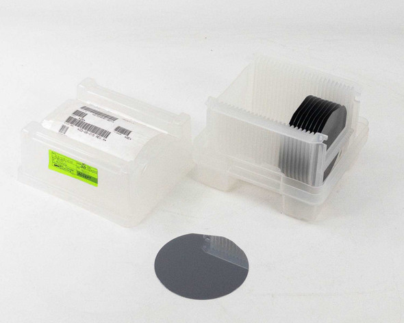
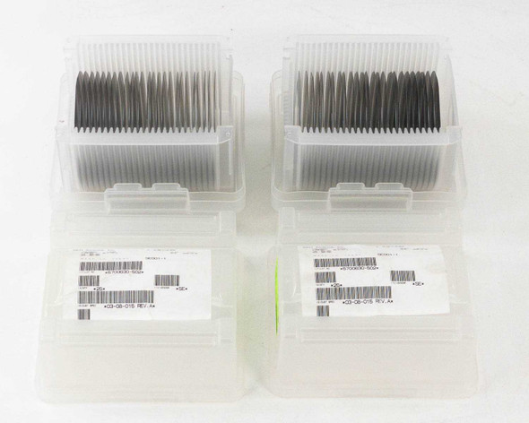
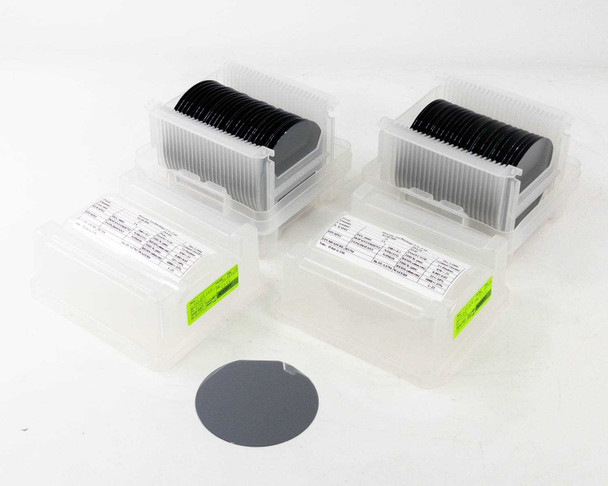
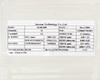
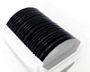
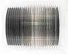
These Atecom Technology 100mm N/PHOS polished silicon wafers (Part# 03-08-008) have been inspected and appear to be in good condition. The wafers are stored in their original plastic cassette carriers — two cassettes of 25 wafers each — and the polished surfaces appear clean and intact with no visible breakage or contamination noted during inspection. The cassette labels are intact and legible, confirming all specification data. These were pulled from a working semiconductor environment. Please view our photo set and contact us if you have any questions.
Warranty Information
Additional Information
Brand: |
Atecom Technology |
Model: |
03-08-008 |
MPN: |
03-08-008 |
Type: |
Polished Silicon Wafer |
SKU: |
53136 |
Quantity: |
50 wafers (2 cassettes of 25) |
Diameter: |
100mm (+/-0.5mm) |
Thickness (Substrate): |
450 µm +/-25 µm |
Thickness (Epi Layer): |
22 µm +/-10% |
Resistivity (Substrate): |
0.005–0.02 ohm-cm |
Resistivity (Epi Layer): |
1000 +/-25% ohm-cm |
Dopant / Conductivity Type: |
N-Type / Phosphorus (N/PHOS) |
Orientation: |
(111) — N/Sb/(111) substrate |
Wafer Surface: |
Polished |
EPI Run#: |
06-111-A3792 (Cassette 1A), 06-111-A3794 (Cassette 2A) |
Wafer # Range: |
1–25 per cassette |
Date of Manufacture: |
December 5, 2006 |
Inspector: |
Li Jianhua |
PO Number: |
O200607281001 |
Condition: |
Used – Pulled from Working Environment |
Seller Notes: |
Lot of 50 wafers in two sealed plastic cassettes of 25 each |
Country/Region of Manufacture: |
Taiwan |
Application / Use Case: |
Epitaxial substrate, semiconductor R&D, device fabrication |
Form Factor: |
100mm (4-inch) wafer cassette |
Condition Notes: |
Atecom 100mm N/PHOS silicon wafers (03-08-008), lot of 50. Inspected and in good condition. Stored in original cassettes, polished surfaces appear clean and intact. Pulled from a working semiconductor environment. |