
Atecom Technology
-
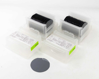

Atecom 100mm P-Type Silicon Wafers 525±25µm 1250±20% Ωcm B/100 Epi Qty 50
Atecom Technology
$500.00Was: $1,000.00Atecom 100mm P-Type Silicon Wafers 525±25µm 1250±20% Ωcm B/100 Epi Qty 50Lot of 50 epitaxial polished silicon wafers manufactured by Atecom Technology. P-type boron-doped substrate with epitaxial...53137- SKU:
- 53137
- Availability:
- Usually ships within 1-2 business days.
- Weight:
- 6.00 LBS
- Brand:
- Atecom Technology
- Model:
- 03-09-009
- MPN:
- 03-09-009
- Type:
- Epitaxial Polished Silicon Wafer
- SKU:
- 53137
- Quantity:
- 50 wafers (2 cassettes of 25)
- Diameter:
- 100mm (4 inch)
- Thickness:
- 525 ±25 µm (substrate)
- Resistivity:
- 1250 ±20% Ωcm (epi layer)
- Conductivity Type:
- P-Type
- Dopant:
- Boron (B₂H₆)
- Crystal Orientation:
- (100) / 1-0-0
- Dopant/Orient (Sub Spec):
- P/Boron/(100)
- Epi Type/Dopant:
- P/B₂H₆
- Epi Layer Thickness:
- 85 ±10% µm
- Sub Spec Resistivity (Ωcm):
- 0.01-0.02
- Sub Spec Diameter:
- 100 ±1.0 mm
- Epi Run Numbers:
- 06-II-B1078 (Cassette 1B), 06-II-B1081 (Cassette 2B)
- Date of Manufacture:
- July 11, 2006
- PO Number:
- O200605081003
- Surface:
- Polished
- Condition:
- Used – Inspected and Tested
- Seller Notes:
- Lot of 50 wafers in two plastic cassettes of 25 each with original Atecom spec labels
- Country/Region of Manufacture:
- Taiwan
- Application:
- Semiconductor research, MEMS, photovoltaics, epitaxial device fabrication
- Form Factor:
- Wafer / Substrate
- Compatible With:
- Standard 100mm (4-inch) wafer process equipment and cassettes
- Condition Notes:
- Atecom 100mm P-type epi silicon wafers, lot of 50. Inspected and in good condition. Stored in original plastic cassettes with spec labels intact. Pulled from a working environment. Please contact us with any questions.
- California Prop 65 Warning:
- WARNING: This product can expose you to chemicals including lead and lead compounds, and DEHP (a phthalate), which are known to the State of California to cause cancer and birth defects or other reproductive harm. Go to P65Warnings.ca.gov
$500.00Was: $1,000.00 -


Atecom 100mm Silicon Wafer N/PHOS 450µm 1000 Ohm-cm (111) 03-08-008 Qty 50
Atecom Technology
$675.00Was: $1,400.00Atecom 100mm Silicon Wafer N/PHOS 450µm 1000 Ohm-cm (111) 03-08-008 Qty 50Lot of 50 polished 100mm silicon wafers with N-type phosphorus doping. These epitaxial substrates feature a highly doped...53136- SKU:
- 53136
- Availability:
- Usually ships within 1-2 business days.
- Weight:
- 6.00 LBS
- Brand:
- Atecom Technology
- Model:
- 03-08-008
- MPN:
- 03-08-008
- Type:
- Polished Silicon Wafer
- SKU:
- 53136
- Quantity:
- 50 wafers (2 cassettes of 25)
- Diameter:
- 100mm (+/-0.5mm)
- Thickness (Substrate):
- 450 µm +/-25 µm
- Thickness (Epi Layer):
- 22 µm +/-10%
- Resistivity (Substrate):
- 0.005–0.02 ohm-cm
- Resistivity (Epi Layer):
- 1000 +/-25% ohm-cm
- Dopant / Conductivity Type:
- N-Type / Phosphorus (N/PHOS)
- Orientation:
- (111) — N/Sb/(111) substrate
- Wafer Surface:
- Polished
- EPI Run#:
- 06-111-A3792 (Cassette 1A), 06-111-A3794 (Cassette 2A)
- Wafer # Range:
- 1–25 per cassette
- Date of Manufacture:
- December 5, 2006
- Inspector:
- Li Jianhua
- PO Number:
- O200607281001
- Condition:
- Used – Pulled from Working Environment
- Seller Notes:
- Lot of 50 wafers in two sealed plastic cassettes of 25 each
- Country/Region of Manufacture:
- Taiwan
- Application / Use Case:
- Epitaxial substrate, semiconductor R&D, device fabrication
- Form Factor:
- 100mm (4-inch) wafer cassette
- Condition Notes:
- Atecom 100mm N/PHOS silicon wafers (03-08-008), lot of 50. Inspected and in good condition. Stored in original cassettes, polished surfaces appear clean and intact. Pulled from a working semiconductor environment.
- California Prop 65 Warning:
- WARNING: This product can expose you to chemicals including lead and lead compounds, and DEHP (a phthalate), which are known to the State of California to cause cancer and birth defects or other reproductive harm. Go to P65Warnings.ca.gov
$675.00Was: $1,400.00